
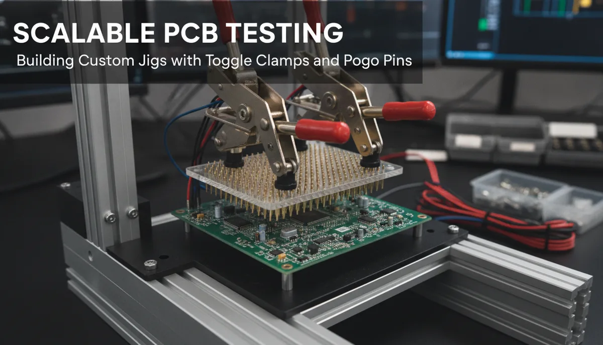
Scalable PCB Testing: Building Custom Jigs with Toggle Clamps and Pogo Pins
In the transition from a single prototype to a small production run, the most significant hurdle is rarely the soldering itself—it is the verification. For many makers and hardware engineers, the "testing phase" involves a tedious cycle of plugging in a USB cable, waiting for a bootloader, flashing firmware, checking serial output, and then unplugging.
When you are making five boards, this is a minor annoyance. When you are making fifty or five hundred, it becomes a physical and temporal bottleneck. James Bowman of Excamera Labs recently highlighted a solution to this exact problem: "the machine for making the machine." By utilizing quick-release toggle clamps and specialized contact points, you can move away from manual handling and toward a streamlined, professional testing workflow.
The Production Bottleneck: Why Manual Testing Fails
The primary enemy of efficient hardware production is friction. Manual testing introduces friction in three specific ways:
- Connector Wear: Micro-USB and even USB-C ports have a finite cycle life. Repeatedly plugging and unplugging cables during testing can fatigue the solder joints or the internal pins of the connector before the product even reaches the customer.
- Temporal Inefficiency: The physical act of aligning a cable and ensuring it is seated takes several seconds. Multiplied by hundreds of units, this represents hours of wasted labor.
- Inconsistency: Manual testing relies on the human operator to notice failures. If a cable isn't fully seated, a board might fail a test not because of a defect, but because of a poor connection, leading to "false negatives" that require troubleshooting.
To scale effectively, you need a system that standardizes the connection. This is where the concept of the test jig—specifically one utilizing toggle clamps—becomes essential. For those looking to upgrade their entire production environment, The Soldered Anywhere Master Buying Guide offers a broader look at the tools required for a professional-grade bench.
Anatomy of a Professional Test Jig
A test jig is essentially a mechanical interface that translates a simple physical motion (like flipping a lever) into multiple precise electrical connections. The core components of a modern DIY jig include:
Quick-Release Toggle Clamps
As noted in the Excamera Labs project, toggle clamps are the muscle of the machine. These clamps move a shaft linearly or in an arc to apply downward pressure. In a testing context, the clamp doesn't just hold the board; it pushes the board (or a contact plate) onto a bed of spring-loaded pins.
US Stock 225D Horizontal Quick-R...
Pogo Pins (Spring-Loaded Contacts)
Pogo pins are the unsung heroes of the electronics industry. These are small, gold-plated tubes containing a spring and a plunger. When the toggle clamp is engaged, the pogo pins compress against the test points (TP) or via pads on your PCB. This creates a low-resistance electrical connection without needing to solder a single header.
The Alignment Frame
The "machine" requires absolute precision. If your pogo pins are off by even half a millimeter, they may miss the test points or cause a short circuit. Most professional jigs use a combination of CNC-milled acrylic or 3D-printed guides to ensure the PCB sits in the exact same spot every time.
Designing Your PCB for Testability
You cannot build an efficient test jig if the PCB itself isn't designed for it. This is a concept known as Design for Test (DFT). When laying out your board in KiCad or Altium, consider the following:
- Dedicated Test Points: Avoid trying to hit the legs of SMD components. Instead, place 1mm circular pads on the bottom of the PCB. These pads provide a flat, stable surface for pogo pins.
- Alignment Holes: Include at least two non-plated mounting holes on opposite corners of your PCB. These holes fit onto "alignment pins" on your jig, ensuring the board cannot shift during the clamping process.
- Single-Side Access: Whenever possible, place all test points on the bottom of the board. This allows for a "bed of nails" style jig where the board is simply pressed down onto the pins, leaving the top side accessible for visual inspection or interacting with buttons.
For complex projects involving data logging, such as Wireless LCD Streaming for the ANENG AN870: A Deep Dive into Multimeter Hacking, having reliable test points is the difference between a successful data stream and a frustrated afternoon of signal hunting.
Step-by-Step: Building a Toggle-Clamp Test Jig
Building a jig doesn't require a machine shop. With a 3D printer and some basic hardware, you can assemble a functional "machine for making the machine" in a weekend.
1. The Base Plate
Start with a rigid base. While 3D-printed plastic works for the frame, the base that holds the pogo pins should ideally be something that won't warp under pressure, such as a thick acrylic sheet or a FR4 fiberglass board.
2. Installing the Pogo Pins
Drill holes in your base plate that match your PCB's test point layout. Press-fit the pogo pin sockets into these holes. Using sockets rather than soldering the pins directly to the base allows you to replace broken or worn pins easily.
3. Mounting the Toggle Clamp
Position the toggle clamp so that its plunger hits the center of the PCB (or a secondary "pressure plate" that distributes the force). You want enough pressure to compress all pogo pins by about 50-75% of their travel.
4. Wiring the Interface
The "back end" of your pogo pins should be wired to your testing hardware. This might be an Arduino, a Raspberry Pi, or a dedicated programmer like an ESP-Prog. By connecting the jig to a computer, you can automate the entire process: clamp the board, the computer detects the connection, flashes the firmware, runs a self-test, and lights up a green LED if it passes.
Advanced Integration: Automation and Software
The true power of a toggle-clamp jig is realized when it is paired with an automated test script. Instead of manually checking if a board works, your jig can perform "In-Circuit Testing" (ICT).
For example, your script can:
- Measure the resistance between power rails to check for shorts before applying power.
- Check the voltage levels of onboard regulators.
- Communicate via I2C or SPI to verify that peripheral sensors are responding.
This level of rigor is what separates hobbyist projects from professional-grade hardware. If you find yourself needing to perform repairs in the field before a jig-tested batch is ready, refer to our guide on Emergency RC Repair: Soldering in the Pits for tips on high-stakes soldering.
Conclusion: Investing in the Process
As James Bowman demonstrated, the "machine for making the machine" is an investment in your own productivity. While it takes time to design and assemble a custom test jig, the ROI is immediate. You save your connectors from wear, you eliminate the variability of manual cables, and you gain the confidence that every board leaving your bench has been rigorously and consistently tested.
Whether you are building a simple breakout board or a complex colorimeter—like the one we explored in Beyond the Data Sheet: Hacking the CR4501 Colorimeter for RAL Support—a dedicated test jig is the hallmark of a mature engineering workflow. Stop plugging in cables and start clamping down on quality.
Related product: US Stock 225D Horizontal Quick-R...