
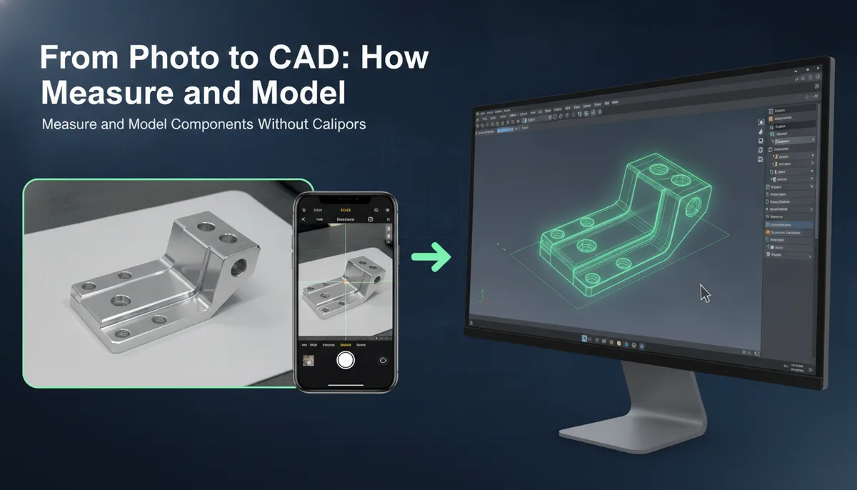
From Photo to CAD: How to Measure and Model Components Without Calipers
The "Part-in-Hand" Paradox: Designing Before the Mail Arrives
Every maker knows the frustration of the "design stall." You have a brilliant idea for a handheld project, you’ve ordered the microcontrollers and sensors, but they won't arrive for three days. You want to start 3D modeling the enclosure now so you can hit "print" the moment the components land, but you don't have the physical parts to measure with your calipers.
Common wisdom says you need the datasheet or the physical part to proceed. However, datasheets for hobbyist components can be notoriously sparse, often omitting the exact placement of a mounting hole or the specific radius of a PCB corner.
The good news is that you don’t need calipers, a datasheet, or even the real part to determine precise component dimensions. By leveraging high-quality product photography and the basic "box dimensions" listed on retail sites, you can use FreeCAD to "reverse engineer" a 1:1 scale model that is accurate enough for professional-grade enclosures.
Why Product Photos are a Maker’s Secret Weapon
Not all photos are created equal. To model a part accurately, you need an orthographic—or "flat"—representation. Perspective is the enemy of measurement; if a photo is taken at an angle, the far side of the PCB will appear smaller than the near side, throwing off your scale.
Retailers like Adafruit are a goldmine for this workflow because their product photography is exceptionally high quality. They often provide "top-down" shots taken with long focal lengths, which flattens the image and minimizes parallax distortion. When you combine these clear visuals with the "Product Dimensions" section usually found at the bottom of the page, you have everything you need to begin.
Before you start, ensure you have a clean save of the highest-resolution photo available. In the world of the Soldered Anywhere Master Buying Guide, we often emphasize having the right tools for the job—and in the digital realm, a high-resolution JPG is as essential as a good soldering iron.
Setting Up FreeCAD for Image Calibration
FreeCAD features a powerful, often overlooked toolset for handling 2D images. To begin, you’ll need to move away from the standard Part Design workbench momentarily.
Step 1: Importing the Image
Open FreeCAD and create a new document. Switch to the Image Workbench. Click the "Create an image in the 3D space" icon and select your saved product photo. You will be prompted to select a plane; for a top-down PCB shot, the XY-Plane (Top) is usually the best choice.
Step 2: The Calibration Magic
This is the most critical step. Your imported image has no real-world scale yet; FreeCAD just sees it as a collection of pixels.
- Select the image object in the tree view.
- Look for the Calibration tool (it looks like a small ruler over a picture).
- Click two points on the image that correspond to a known dimension. For example, if the Adafruit product page says the PCB is exactly 50mm long, click the far left edge and the far right edge of the PCB in the photo.
- A dialog box will appear asking for the distance. Type "50mm".
Instantly, FreeCAD scales the entire image so that those two points are exactly 50mm apart in 3D space. Every other pixel in that photo now represents a real-world measurement.
Step-by-Step: From Pixels to Geometry
Once calibrated, you can switch to the Sketcher Workbench to begin tracing. This is where the workflow turns from observation into engineering.
Tracing the Perimeter
Create a new sketch on the same plane as your image. You will see the photo sitting behind your grid. Use the polyline tool to trace the outer edge of the PCB. Even if the photo has slight shadows, you can usually identify the "true" edge by looking for the high-contrast line where the green or black solder mask meets the background.
Locating Mounting Holes
This is where the photo-method shines. Measuring the center-to-center distance of mounting holes with calipers can be finicky. In FreeCAD, you can simply place a circle over the hole in the photo. If the hole looks slightly oblong due to a minor camera angle, center your circle on the hole's footprint.
150 x 0.1mm Electronic Digital C...
Modeling Component Height
While the top-down photo gives you X and Y coordinates, you still need the Z-axis (height). For this, look for a side-profile photo on the product page. You can repeat the calibration process on the XZ plane to determine the height of tall components like electrolytic capacitors or USB-C ports. This ensures that when you design your enclosure, the lid won't crush your hardware.
Ensuring Accuracy: The Limitations of Optical Measurement
While this method is incredibly effective, it is not magic. You must account for a few technical realities:
- Parallax: Even the best photos have some perspective. If you are modeling a thick component (like a terminal block), the top of the block will appear slightly shifted compared to the pins where they meet the PCB. Always trace the footprint at the PCB level for the most accurate fit.
- Lens Distortion: Cheaper cameras use wide-angle lenses that "bow" the image (barrel distortion). If the straight edges of a PCB look curved in the photo, your measurements will be off. Stick to professional photos from reputable sources.
- The 0.2mm Rule: When 3D printing an enclosure based on a photo-modeled part, always add a "slop" or tolerance factor. Adding 0.2mm to 0.5mm of extra space around your traced lines will account for both modeling inaccuracies and the expansion of 3D printer filament.
If you are modeling something complex, like the Pinecil V2, you might find that the ergonomic curves are harder to capture from a single photo. In these cases, using multiple photos from different angles (Top, Side, Front) and calibrating each one is the key to success.
Application: Designing Enclosures and Footprints
Why go through this trouble? Beyond just "pre-designing" while waiting for shipping, this method allows you to create custom PCB footprints for software like KiCad when a library doesn't exist.
Imagine you are hacking a tool like the ANENG AN870 multimeter, as discussed in our guide on Wireless LCD Streaming for the ANENG AN870. If you need to design a custom bracket to hold an ESP32 against the multimeter's internal PCB, you can simply take a high-quality photo of the multimeter's guts, drop it into FreeCAD, and design a bracket that fits the internal ribs and screw bosses perfectly.
This technique bridges the gap between "eyeballing it" and expensive 3D scanning. It turns your screen into a virtual workbench where the parts are always in stock and the measurements are just a click away.
Conclusion: Expanding Your Design Toolkit
The ability to measure from photos transforms how you approach project planning. It removes the "dead time" spent waiting for components to arrive and allows for a more fluid, integrated design process.
By mastering the Image workbench in FreeCAD, you aren't just tracing pictures; you are utilizing photogrammetry principles to speed up your workflow. Whether you're building a rugged case for a field-repair kit or a sleek desktop gadget, the combination of high-quality retail photography and FreeCAD’s calibration tools is a superpower for the modern maker.
Next time you’re browsing a part on Adafruit, don’t just look at the specs—save the photo. Your future CAD model will thank you.
Related product: 150 x 0.1mm Electronic Digital C...